555 Astable Mode: Generating Square Waves
Electrical Diagrams · made in Skemio
What it shows
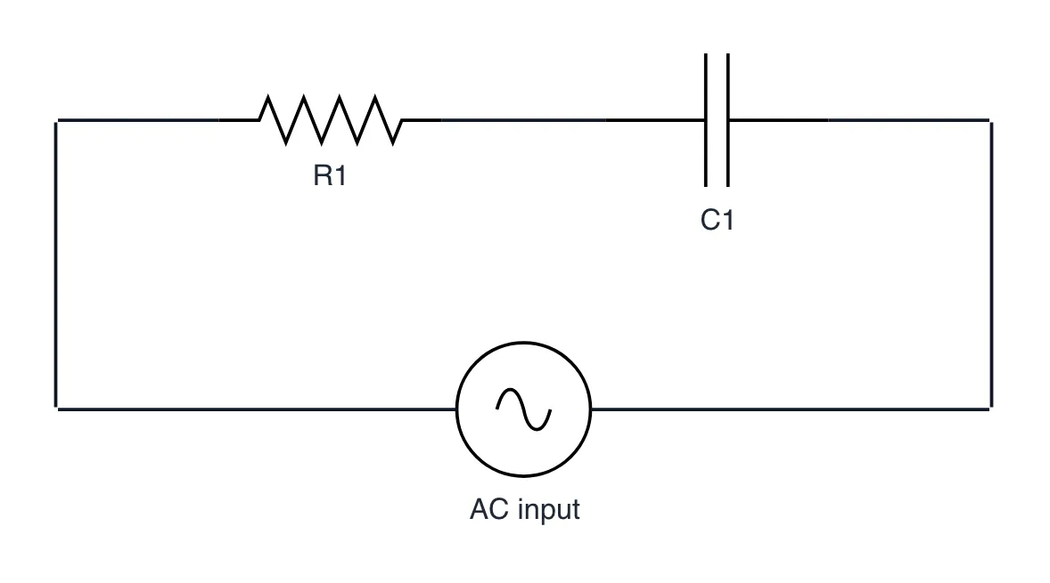
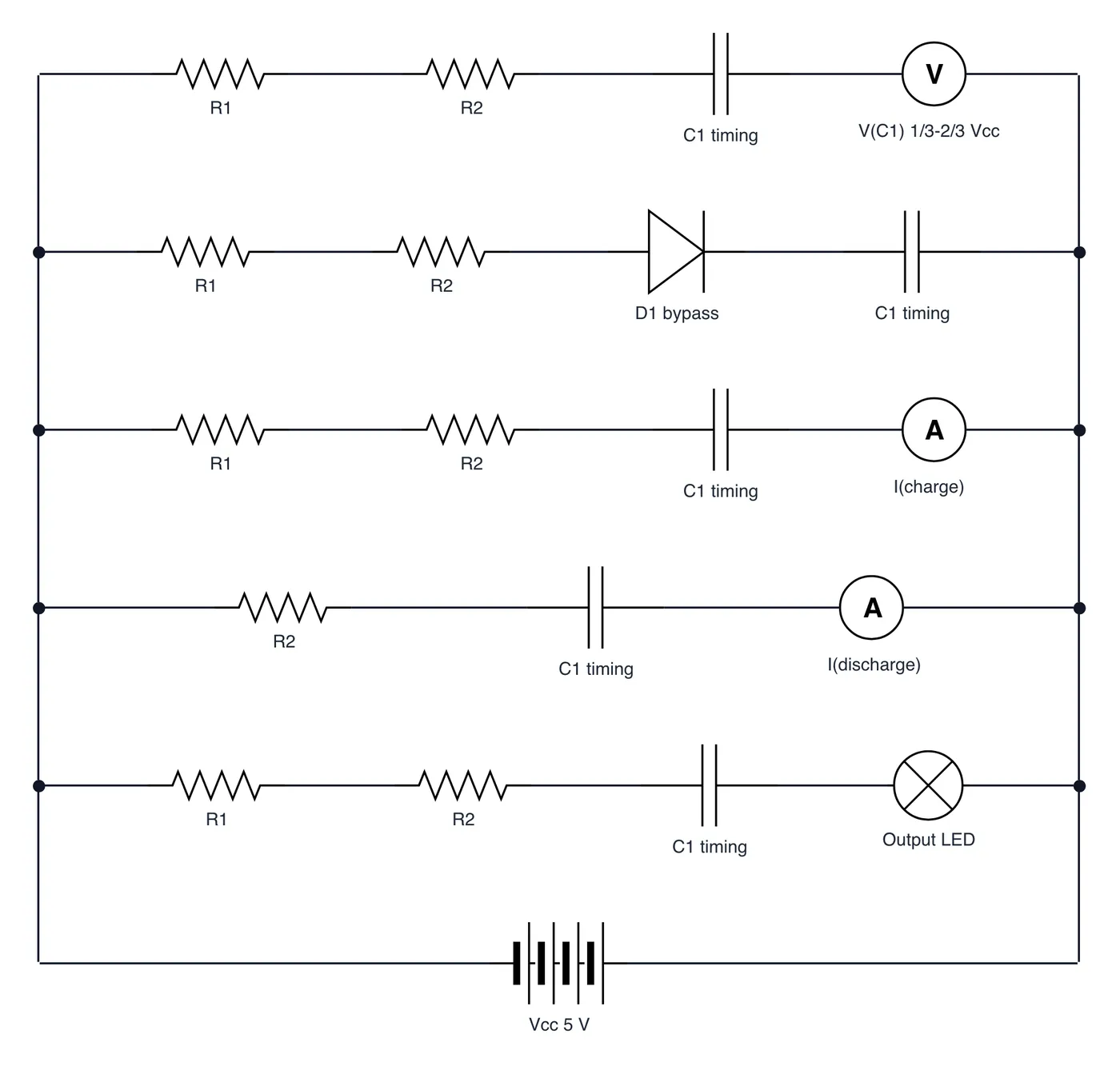
- Timing capacitor charges between 1/3 Vcc and 2/3 Vcc reference thresholds.
- Charge path flows through R1 + R2; discharge path flows solely through R2.
- Output duty cycle is fundamentally always greater than 50% without a bypass diode.
The takeaway
The 555 astable alternates between 1/3 and 2/3 Vcc thresholds, setting frequency purely via R1, R2, and C1.
- #555Timer
- #Circuits
- #Electronics
- #DIYElectronics
- #Maker